Understanding the internal design of a TK-905-4G
July 14th, 2023, last changes on December 7th, 2023Schematics
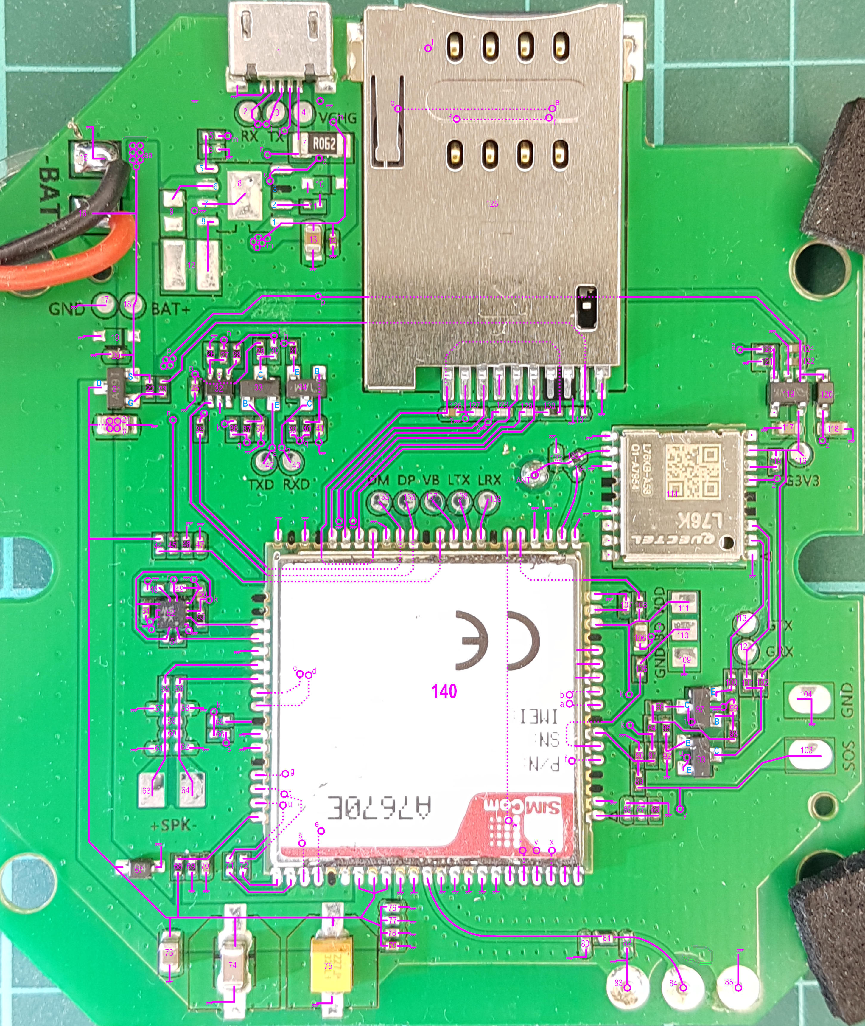
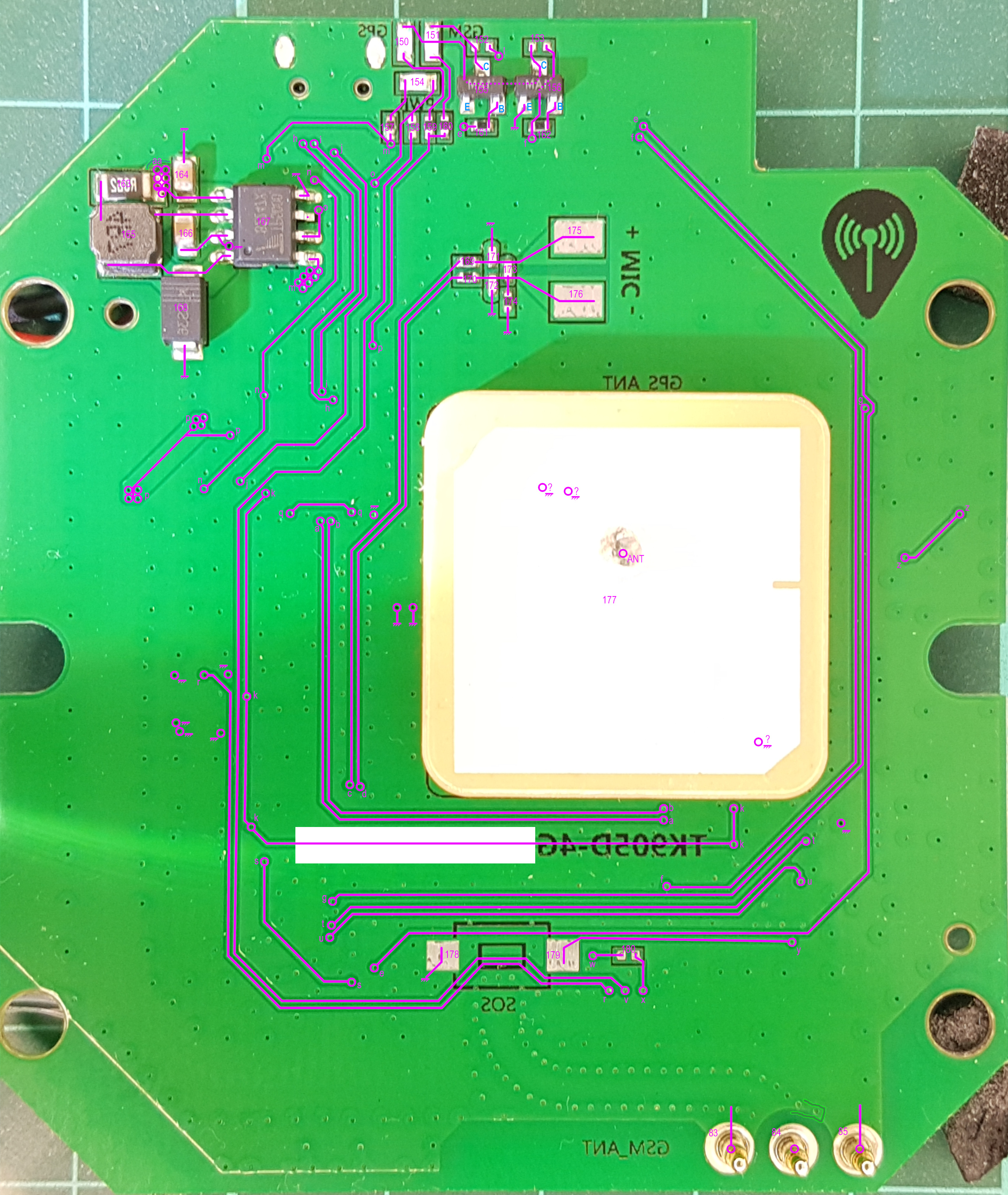
You may find photos of the PCB, including marked paths and numbered elements, as well as a schematic. Please note, some of the connections are either not visible or impossible to get clearly measured without destroying the device. The passive components are not measured. It may happen that some resistors are mixed with capacitors or vice-versa. Any corrections/suggestions are highly welcome!
Notation used:
- On the photos, components and test points are simply enumerated from 1 to 140 (front side) and from 150 to 180 (back side).
- The through holes are enumerated by letters and kept same for the same wire along the whole PCB (from a to z, aa).
- Uncertain connections (guessed or measured) are drawn dotted-line.
- Blue circles (on the schematics) denote unknown wiring from the marked point on.
- The schematic uses standard reference designators (for as long as possible) followed by a number as on the PCB photos:
- AE for antennas
- BT for a battery
- C for capacitors
- D for diodes (including LEDs)
- e for unpopulated components (non-standard)
- J for connectors
- L for inductors
- LS for speaker
- P for the SIM-Card socket
- Q for transistors
- R for resistors
- TP for test points
- U for integrated circuits
- X as a prefix for the through-hole identifiers (letters)
PCB Photos
Note: the back side is mirrored for a simpler match
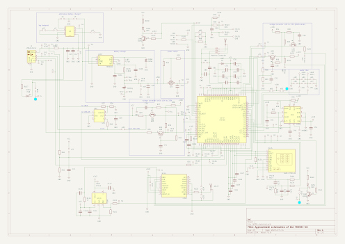
PCB Schematics
Antenna Short-Circuit?
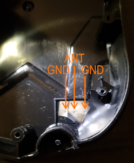
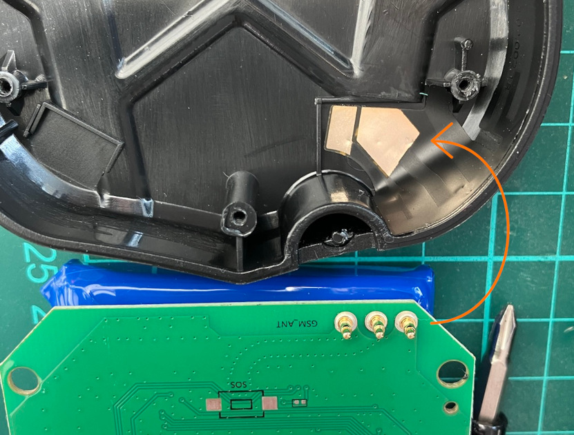
The antenna is a flexible PCB glued into the housing. Three spring jumpers do a connection from the PCB to the antenna: two outer ones are GND, the middle one is the signal. Update: Two of my units give a short-circuit between the signal and the GND as on the picture. It seems, it's designed this way. But why? And how does it work (not only destroying the transmitter, but also getting a reasonable cellular connection).
USB and Serial Port
The wiring of the USB port is nothing like standard:
- The ID pin can be used to send serial data to the modem (routed via a voltage converter to 1.8V domain of the modem).
- The D- pin is wired to the USB_DM pin of the modem (via a resistor), which seems to be fine.
- The D+ pin is wired to a S7D chip (more below).
- The VBUS is used indeed to charge the battery, as well to give a high state to the S7D chip, and via a voltage divider to the ADC pin of the modem (why?).
It looks like the intention was to use the D+ pin to get serial data from the modem, but there is a gap e30 making it impossible. Anyway, there is a fully functional voltage converter from 1.8V domain to 3.8V domain. Unused.
I was considering the S7D chip could be a tri-state digital buffer, switching between the serial line and the real USB protocol, but the wiring does not seem to support it. Still, a few connections are not visible: I had to measure them with a multimeter - maybe there is some mistake.
Battery charger
There is a simple battery charger based on the TP5000X chip, doing it's job. It looks like there is an alternative circuit (not populated) for a charging function as well (chip U8 on the schematics).
The red LED is controlled by the battery charger.
Power Switch
The power is switched on by inserting a SIM card. This opens the P-Channel MOSFET (Q21) and provides ca. 3.8V to the circuit (to the modem, to the GNSS receiver via a 3.3V LDO, to the accelerometer via the modem and to the S7D chip).
GNSS Receiver
The unit uses an external GNSS receiver (L76K, U114), communicating with the modem via a serial protocol. An appropriate voltage converter is realized using transistors. An unpowered GNSS antenna is located on the back side of the PCB.
Accelerometer
The unit uses an external accelerometer (to detect vibrations). It seems to be identical to Bosch BMA456 chip and communicating over the I2C protocol with the modem, generating interrupt on move (pin 5 of the X4SW chip, pin 67 of the modem).
3.3V LDO
The chip P1VK (U119) is a 3.3V LDO. The pin functions are estimated.
LTE Modem
As an LTE modem a SIMCom A7670E module was used. The PCB seems to be prepared for other compatible modules, e.g. a one incorporating a GNSS receiver. The chip used does not provide an analogue speaker output and analogue microphone input. Still, most of the wiring is in place.
Provisions
The PCB provides wiring for a speaker (unpopulated), for a microphone (populated but no microphone) and an SOS button. Unfortunately, the modem chip does not offer analogue signals, therefore this function can't be easily extended. The SOS input seems to be ignored by the device, which means a firmware modification would be needed to make use of this function.
Data Flow Analysis
Note: for privacy some data has been X-ed
TX line
Bye bye bootloader
LTX Line
Update: Data is transmitted at 115200 bps, 8 bit data, no parity, 1 stop bit.
[INFO: CPU       ] CHIP_ID: 0x1603, REV_ID: 0xA3
[INFO: CPU       ] PLATFORM: CRANEM (SILICON)
[INFO: Main      ]
[INFO: Main      ] Starting AROM-CRANE (Version: XXXX.XX.XX)
[INFO: Qspi      ] QSPI clock configured at 13 MHz
[INFO: QspiFlash ] Detecting QSPI flash devices...
[INFO: QspiFlash ] Found a known spi flash device "XM25QU128C"
[INFO: QspiFlash ] SPI nor flash: Manufacturer ID: 0x20, Device ID: 0x4118
[INFO: UbiSimple ] Detected peb size is 4096, the first good peb number is 0
[INFO: Crypto    ] Initializing crypto library...
[INFO: Main      ] Running in normal booting mode.
[INFO: Main      ] Loading...
[INFO: Bl1Main   ] Welcome to boot rom.
[INFO: Bl1Main   ] ### Non-trusted boot mode. ###
[INFO: Bl1Main   ] Found preboot volume, size is 26660 bytes
[INFO: Bl1Main   ] BL1: Trying to load and verify BL2 image from volume preboot...
[INFO: Bl1Main   ] BL1: OKay.
[PRI : Preboot   ] Executing preboot application...
[PRI : Preboot   ] Preboot version: XXXX.XX.XX
[PRI : Preboot   ] Usb phy reg 29 0x0 -> 0x0
[PRI : PMIC      ] Found PMIC with Id: 0x18
[PRI : Preboot   ] Power_up_reason=0x2.
[PRI : Preboot   ] Power_down_reason=0x0.
[WARN: Preboot   ] Warning: power_up_reason unknown.
[PRI : Psram     ] [PSRAM] psram init CraneG, phy100_wb67_ap100 .
[PRI : Psram     ] WB_250MHZ_8M8M
[PRI : EFuse     ] No embedded flash
[PRI : Psram     ] flush_idle @[0xXXXXXXXX]=[0xF0000200]
[PRI : Psram     ] dis_psc_ckagate @[0xXXXXXXXX]=[0x80000000]
[INFO: Bl1Main   ] Found bootloader volume, size is 38840 bytes
[INFO: Bl1Main   ] BL1: Trying to load and verify BL2 image from volume bootloader...
[INFO: Bl1Main   ] BL1: OKay.
[PRI : Boot2     ] Executing boot2 application...
[PRI : Boot2     ] Boot2 version: XXXX.XX.XX
Boot33 UART INIT DONE
[BOOT33]VB_VERSION_DATE   :[XXXXXXXX]
PowerOnLog: 0x2
Built by DS-5.
boot33 MPU config
>>>>>>>>>>>>>>>>>>>>>>>>>>>>>>>>>>>>>>>>>>>>
 B33 JUMP TO LOGO at 0xXXXXXXXX
>>>>>>>>>>>>>>>>>>>>>>>>>>>>>>>>>>
 ********************************************
 ** BOOTLOADER DONE JUMP TO CP IMAGE
 ** VERSION : XXXXXXXX
 ** PC      : 0x80040000
 ********************************************
[00]
GRX line
Communication from the modem to the GNSS unit. Seems to be used for configuration only, e.g., the geofence request is not transmitted to the GNSS. Update: Data is transmitted at 9600 bps, 8 bit data, no parity, 1 stop bit.
$PCAS03,1,1,1,1,1,1,1,1,0,0,,,0,1*03
AGNSS data from CASIC.
DataLength: 2746.
Limitation: 7966/50000.
The command does mean: enable GGA, GLL, GSA, GSV, RMC, VTG, ZDA, ANT sentence output in NMEA output. Following lines are no valid commands.
GTX line
Data repored by the GNSS unit. Update: Data is transmitted at 9600 bps, 8 bit data, no parity, 1 stop bit.
$GPTXT,01,01,02,MA=CASIC*27
$GPTXT,01,01,02,IC=AT6558R-XX-XX-XXXXXXXX*XX
$GPTXT,01,01,02,SW=URANUS5,VX.X.X.X*XX
$GPTXT,01,01,02,TB=XXXX-XX-XX,XX:XX:XX*XX
$GPTXT,01,01,02,MO=GB*77
$GNGGA,,,,,,0,00,25.5,,,,,,*64
$GNGLL,,,,,,V,N*7A
$GNGSA,A,1,,,,,,,,,,,,,25.5,25.5,25.5,1*01
$GNGSA,A,1,,,,,,,,,,,,,25.5,25.5,25.5,4*04
$GPGSV,1,1,00,0*65
$BDGSV,1,1,00,0*74
$GNRMC,,V,,,,,,,,,,N,V*37
$GNVTG,,,,,,,,,N*2E
$GNZDA,,,,,,*56
$GPTXT,01,01,01,ANTENNA OPEN*25

...

$GPTXT,01,01,01,ANTENNA OPEN*25
$GNGST,154110.000,,,,,,,*57
$GNGGA,154110.992,XXXX.XXXXX,X,XXXXX.XXXXX,X,6,04,2.9,-45.3,M,48.3,M,,*XX
$GNGLL,XXXX.XXXXX,X,XXXXX.XXXXX,X,154110.992,A,E*41
$GNGSA,A,3,03,04,06,09,,,,,,,,,6.4,2.9,5.7,1*32
$GNGSA,A,3,,,,,,,,,,,,,6.4,2.9,5.7,4*3F
$GPGSV,3,1,10,01,09,152,,03,46,094,20,04,79,090,21,06,55,294,22,0*6F
$GPGSV,3,2,10,07,08,177,,09,63,224,25,11,14,316,,17,17,230,,0*64
$GPGSV,3,3,10,19,26,247,,31,23,046,,0*68
$BDGSV,1,1,00,0*74
$GNRMC,154110.992,A,XXXX.XXXXX,X,XXXXX.XXXXX,X,5.51,171.37,XXXXXX,,,E,V*XX
$GNVTG,171.37,T,,M,5.51,N,10.21,K,E*17
$GNZDA,154110.992,XX,XX,XXXX,00,00*XX
Design Flaw
Well, one of my units is officially dead now. I believe the flash memory got corrupted as the battery voltage was very low and the unit booted a few times after each other until it got stuck. Only the blue LED stays on, the SIM card seems to get registered (as the SMS messages are being delivered and a phone call gets initiated), but there is no further reaction. Measuring the unit shows that the MCU enables power for the GPS unit. The GPS unit boots correctly and starts sending NMEA messages. But the MCU does not send the previously observed configuration string to the GPS. Instead, after ca. 10 seconds, cuts down the power to the GPS unit and nothing more happens. As I was unlucky asking SIMCom to get any software from them, I can't reprogram the flash by my own. Desoldering the MCU package in order to desolder the flash memory, copy its contents from the working unit and resoldering all again is a no-go in my case.
I belive it's a design flaw as the official document "A7670 Series Hardware Design_V1.00.pdf" says:
It is strongly recommended that the customer use PWRKEY or ‘AT+CPOF’ to shut down, and then power off Vbat (especially when the module does not need to work). In addition, the customer cannot shut down Vbat by disconnecting it, which may cause damage to flash.
If you refer to the approximate schematics (see above) of the device, you will note that both pins PWRKEY and RESET are not design to shut the device down in a gentle way.
Next: Home Automation without a Cloud